Our Journey
We started Laboratory services since Feb-2002 in support to the needs of the industries like semiconductor, engineering, solar, biochemical, R&D, forensic, and many more. Over the years, our highly skilled and experience teams of scientists, engineers, and analysts provides advance nanotechnology services to solve your problems. Since then, Labs-Services has expanded to three(3) fully equipped laboratories, strategically located in Singapore and Malaysia to provide one-stop solution to customers.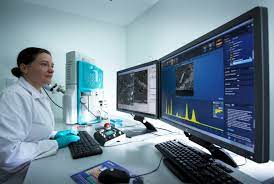

Our Strength
Our diversity origins from our people who possess specific qualifications, hands on know-how and extensive years of experience. Our laboratory is supported not only by lab-personnel, but more importantly it is lead by veterans who are originally from various industries who know your problems well. As for the the equipment and instruments, they are maintained and calibrated by our engineers who are trained by the principal makers, hence we optimise the performance beyond what other laboratory cannot achieve.
Our Commitment
Being the best-in-rank Laboratory in Nanotechnology services, Quasi-S commits to keep every information of our customers in secrecy and confidentiality. All data and reports are under lock-and-key for both soft and hard copies, under strictest protection.
Our Lab Services
Accredited with ISO/IEC 17025 & ISO9001, we are operated by skillful chemists, metallurgist, and lab-technicians. As a one-stop lab-service solution, we can conduct analysis and testing in accordance to international standards such as ASTM, DIN, IEC, JEDEC. In addition, our personnel can be deployed to perform On-Site analysis where situations require. With a special focus on Metallurgy Analysis, we help to provide important information about the structure and properties of metal and alloy samples.
Analysis Capabilities
- IC Interconnect Analysis
- Package deconstruction analysis
- Interfacial structure
- Elemental analysis and mapping
- Microstructure and phase analysis
- Grain structure, grain size distribution (SEM, image analysis)
- Failure interface identification
- Micro-hardness characterization of materials and layers
- Surface roughness
- Metallurgical Testing Service
Analytical Techniques
Physical Analysis
- Optical Microscopy
- Scanning Electron Microscopy (SEM)
- Scanning Transmission Electron Microscopy (STEM)
- Field-Emission Scanning Electron Microscopy (FESEM)
- Transmission Electron Microscopy (TEM)
- Atomic Force Microscopy (AFM)
- Electron Backscatter Diffraction (EBSD)
- Surface Profilometer
- Particle Size Analyser (PSA)
Material Analysis
- Energy Dispersive X-Ray Spectroscopy / Mapping (EDS)
- Fourier Transform Infrared Spectroscopy (FTIR)
- Raman Spectroscopy
- UV-Visible Spectroscopy (UV-VIS)
- Photoluminescence Spectroscopy (PL)
- X-Ray Fluorescence (XRF)
- X-Ray Photoelectron Spectroscopy (XPS)
- Auger Electron Spectroscopy (AES)
- Time-of-Flight Secondary Ion Mass Spectroscopy (TOF-SIMS)
- Electron Energy Loss Spectroscopy (EELS)
- Thermogravimetric Analysis (TGA)
- Differential Scanning Calorimetry (DSC)
Chemical Analysis
- Ion Chromatography (IC)
- Inductively Coupled Plasma Optical Emission Spectroscopy (ICP-OES)
- Inductively Coupled Plasma Mass Spectroscopy (ICP-MS)
- Gas Chromatography Mass Spectroscopy (GC-MS)
- Atomic Absorption Spectroscopy (AAS)
- Volatile Organic Compound (VOC)
- Optical Emission Spectroscopy (OES, Arc Spark)
Mechanical Test
- Brinell Hardness Test
- Rockwell Hardness Test
- Microvicker Hardness Test
- Bend Test
- Tensile Test
- Charpy Impact Test
Non-Destructive Test (In-House)
- Dye Penetrant Crack Test
- Magnetic Particle Crack Test
- In-situ Metallography
- In-situ Hardness Test
Sample Preparation
- Cross-section Preparation
- Biology Sample Preparation (HMDS)
- Sputter Coating
- Chemical Etching
- Ion Milling
- Decapsulation (wet, laser)
- Focused Ion Beam (FIB)
- Reactive Ion Etching (RIE)
Semiconductor Failure Analysis & Reliability Test
- Electrical Verification (I-V, parametric test)
- 2D/3D X-Ray
- Photoemission Microscopy (PHEM)
- Thermal Emission Microscopy (THEM)
- Confocal Scanning Acoustic Microscopy (CSAM)
- Optical Beam Induced Resistance Change (OBIRCH)
- Salt Spray
- Thermal Shock
- Temperature/Humidity Cycling
- Vibration/Mechanical Shock
- High Temperature Oven
- Solderability
Metallurgical Analysis
- Visual Examination
- Macroscopic Examination
- Stereomicroscopic Examination
- Metallography
- Root Cause Investigation
Our Consultation Services
- A method to determine the root cause of failure of a failed or damaged component, device, machinery, equipment or facility.
- The findings provide you with the insight to solve the problem, take remedial action and prevent recurrence.