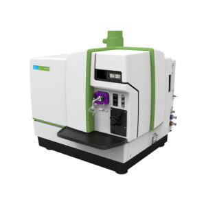
Description
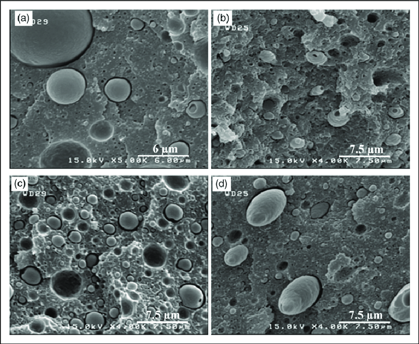
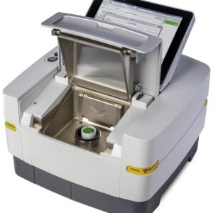
Field Emission Scanning Electron Microscope (FE-SEM) has strong electron source coupled with smaller beam size than a typical SEM. This can magnify the imaging up to 500K times. FE-SEM at Labs-Services is capable of performing high resolution imaging with very low accelerating voltages. With these advantages, observations of super fine features, electron beam sensitive materials, as well as non-conductive materials can be easily achieved.
Applications:
- Ideal microscopic imaging for polymer and thin films.
- Fine corrosion evaluations.
- Micro-structure studies best suitable for R&D
- Detail specimen features’ characterisation.
- Surface contamination elemental analysis
- Material analysis for component layers
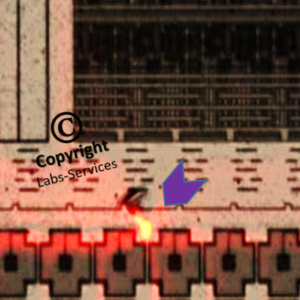
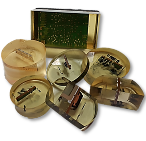
- FA on PCB