Description
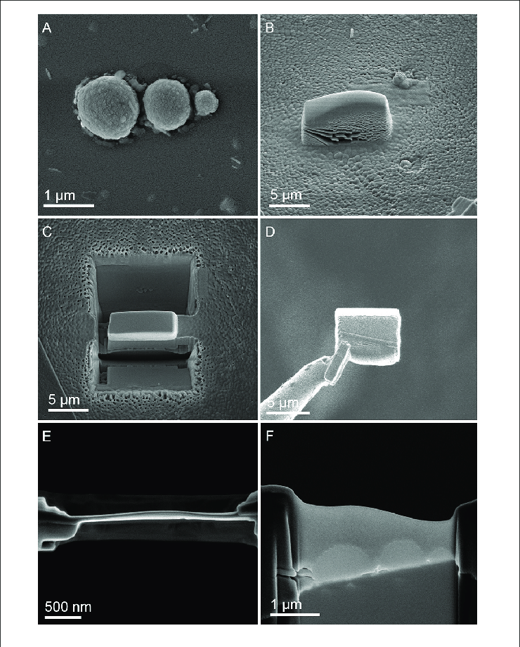
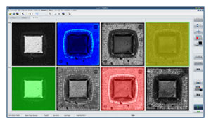
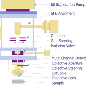
Focused Ion Beam (FIB) is generally used in the semiconductor industry to make modification on semiconductor components like IC etc. It uses a sharp focused beam of gallium ions that can be operated at low beam currents for imaging or high beam currents for site specific sputtering and milling. FIB nowadays can attain below 1 nm imaging resolution. Operation at low beam current, less amount of material is sputtered. But at higher current, a great deal of material can be removed by sputtering, allowing precision milling of the specimen down to a sub-micron scale.
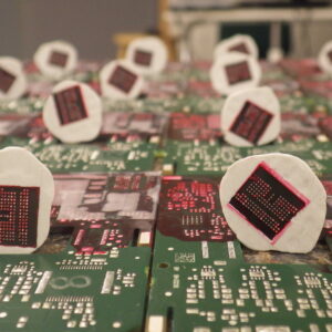
| •SEM, STEM and TEM sample preparation |
| •High resolution cross-section images of small, hard-to-access sample features |