Scanning Electron Microscopy (SEM) magnifies a specific sample region using a high energy focused beam of electrons and have the capability of reaching up to 500,000X.
Unlike others, our SEM has the ability to work under low vacuum without affecting the image quality. It is the most significant advantages when come to inspect non-conductive samples. SEM that operates on high vacuum require samples to be pre-coated with conductive layer, hence distort the natural state of defects.
Stage within the vacuum chamber is large enough to accommodate a normal PCBA board, hence yet again minimizing alteration to the samples. In some cases, we can also perform SEM Analysis in wet condition.

ELEMENTAL DISPERSION SPECTROSCOPY (EDS/EDX)
At this point, a secondary analysis can be performed on the sample region spotted under SEM images. We uses Elemental Dispersion Spectroscopy (EDS) to determine the specific elements that present at the sample region. This method uses X-rays to excite the surface of the sample that gives out energy signature to determine the elements and chemical of selected locations. This combined technique is referred to as SEM-EDS or SEM-EDX Analysis which is very useful in Failure Analysis.
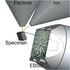
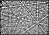
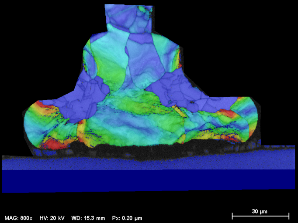
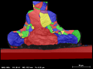
ELECTRON BACKSCATTER DIFFRACTTION (EBSD)
It is a microstructural-crystallographic characterisation technique to study any crystalline or polycrystalline material. The technique involves understanding the structure, crystal orientation and phase of materials in the Scanning Electron Microscope (SEM). Typically it is used to explore microstructures, revealing texture, defects, grain morphology and deformation. It can be combined with complementary techniques within the SEM for phase discrimination.